PIO Program to Control WS2812 LEDs
Now that we have mapped the 1250 ns bit period into instruction cycles, we can implement the PIO program for the WS2812.
We already decided that each bit must occupy a fixed number of cycles, and that the only difference between logic 0 and logic 1 is how many of those cycles the signal remains HIGH. The next step is to arrange PIO instructions so that every transmitted bit follows that cycle pattern.
In this program, we will shift one bit at a time from the TX FIFO and generate the corresponding HIGH and LOW phases by carefully placing instructions and delay slots.
Without side_set
Many WS2812 examples use side_set, including the official Raspberry Pi Pico PIO examples. However, you can also achieve the required timing without using side_set.
After reviewing different implementations, I chose a simpler version that does not use side_set. The timing behavior remains the same; the difference is only in how the pin transitions are expressed in the instructions. This version keeps the logic easier to follow.
Later, we will also look at the side_set based implementation.
PIO Program
Below is the complete PIO program that generates the required WS2812 timing:
set pindirs, 1

.wrap_target
bit_loop:
    set pins, 0 [1]
    out x, 1
    jmp !x do_zero
do_one:
    set pins, 1 [4]
    jmp bit_loop
do_zero:
    set pins, 1 [2]
    set pins, 0 [2]
.wrap
Now let us walk through the program and see how bit value 0 and bit value 1 are generated.
Bitloop starting point:
We begin counting at the start of bit_loop.
set pins, 0 [1]
This instruction takes 2 cycles in total. The pin is driven LOW during these 2 cycles.
Next:
out x, 1
This takes 1 cycle. The pin remains LOW.
Then:
jmp !x do_zero
This also takes 1 cycle, whether the jump is taken or not. The pin is still LOW.
So before we even branch, we have already consumed:
2 + 1 + 1 = 4 cycles
During all 4 of these cycles, the signal is LOW.
From here, execution splits depending on the bit value.
Bit 1 (do_one block):
If the bit in X is 1, the jump is not taken and execution continues into do_one block.
set pins, 1 [4]
This instruction drives the pin HIGH and lasts 5 cycles in total. So the signal stays HIGH for 5 cycles here.
Next:
jmp bit_loop
This takes 1 cycle. The pin is still HIGH during this cycle.
So the total HIGH duration in this path is:
5 + 1 = 6 cycles
Including the 4 LOW cycles at the beginning of the loop, the total bit time is:
4 LOW + 6 HIGH = 10 cycles
Bit 0 (do_zero block):
If the bit in X is 0, the jump goes to do_zero.
We already spent 4 LOW cycles before the branch.
Now we execute:
set pins, 1 [2]
This drives the pin HIGH and lasts 3 cycles in total.
Then:
set pins, 0 [2]
This drives the pin LOW and lasts 3 cycles.
So in this path we have:
Initial LOW = 4 cycles
HIGH = 3 cycles
Final LOW = 3 cycles
Total = 4 + 3 + 3 = 10 cycles
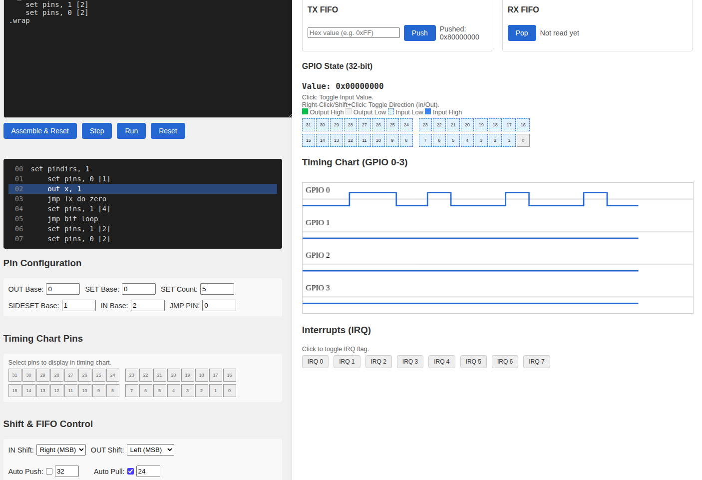
Simulator
Before moving on to the Rust implementation, we can test the program using the PIO simulator: https://ice458.github.io/tools/pio_sim/index.html
To keep things simple, enter the value 0x80000000 as the FIFO input. This value has only the most significant bit set: 1000_0000_0000_0000_0000_0000_0000_0000
That means the very first bit shifted out will be 1, followed by zeros. This makes it easy to clearly observe the waveform difference between a 1 bit and the 0 bits that follow.
If you push the FIFO value without changing any settings, you may not see the waveform for a bit value of 1 immediately. By default, the simulator shifts data from the least significant bit first (right most). In that case, the first 31 bits will be zeros, and the single 1 will appear at the very end.
To match how WS2812 data is transmitted, go to the Shift & FIFO Control section in the simulator and:
- Set OUT Shift to LEFT (MSB)
- Enable Auto Pull
- Set the pull threshold to 24 (since WS2812 data is 24 bits per LED, we pull after 24 bits instead of 32)
The OUT shift direction is important. WS2812 LEDs expect the most significant bit of each color byte to be transmitted first. So shifting left, which sends the MSB first, matches the actual hardware behavior. We are not changing this just for visual convenience; this is how the real device expects the data stream.
With this configuration, you should immediately see one 1-bit waveform followed by 0-bit waveforms.